
Infant Mortality
How a 136-person test equipment company quietly became the toll booth every AI chip has to pass through

Infant Mortality
How a 136-person test equipment company quietly became the toll booth every AI chip has to pass through
At 4:05 PM Eastern on Tuesday, a semiconductor company most people have never heard of closed at $72.01. Ninety minutes later, in after-hours trading, it was pushing toward $95–$100 — up somewhere between 29% and 40% depending on which feed you trust — after posting a fiscal 2027 revenue guide of $130–$150 million against a Wall Street consensus sitting around $85 million. A month earlier, the same stock had touched an all-time high above $126. In between, it had round-tripped down into the high-$60s on nothing more than macro nerves and profit-taking. Same company, same backlog, same customer list — a 40%+ swing in six weeks with no news to justify it either way.
That company is Aehr Test Systems (NASDAQ: AEHR), and the reason its stock behaves like a meme coin with a market cap is actually a pretty boring one: nobody has figured out how to value a monopoly on a process nobody thinks about until it fails.
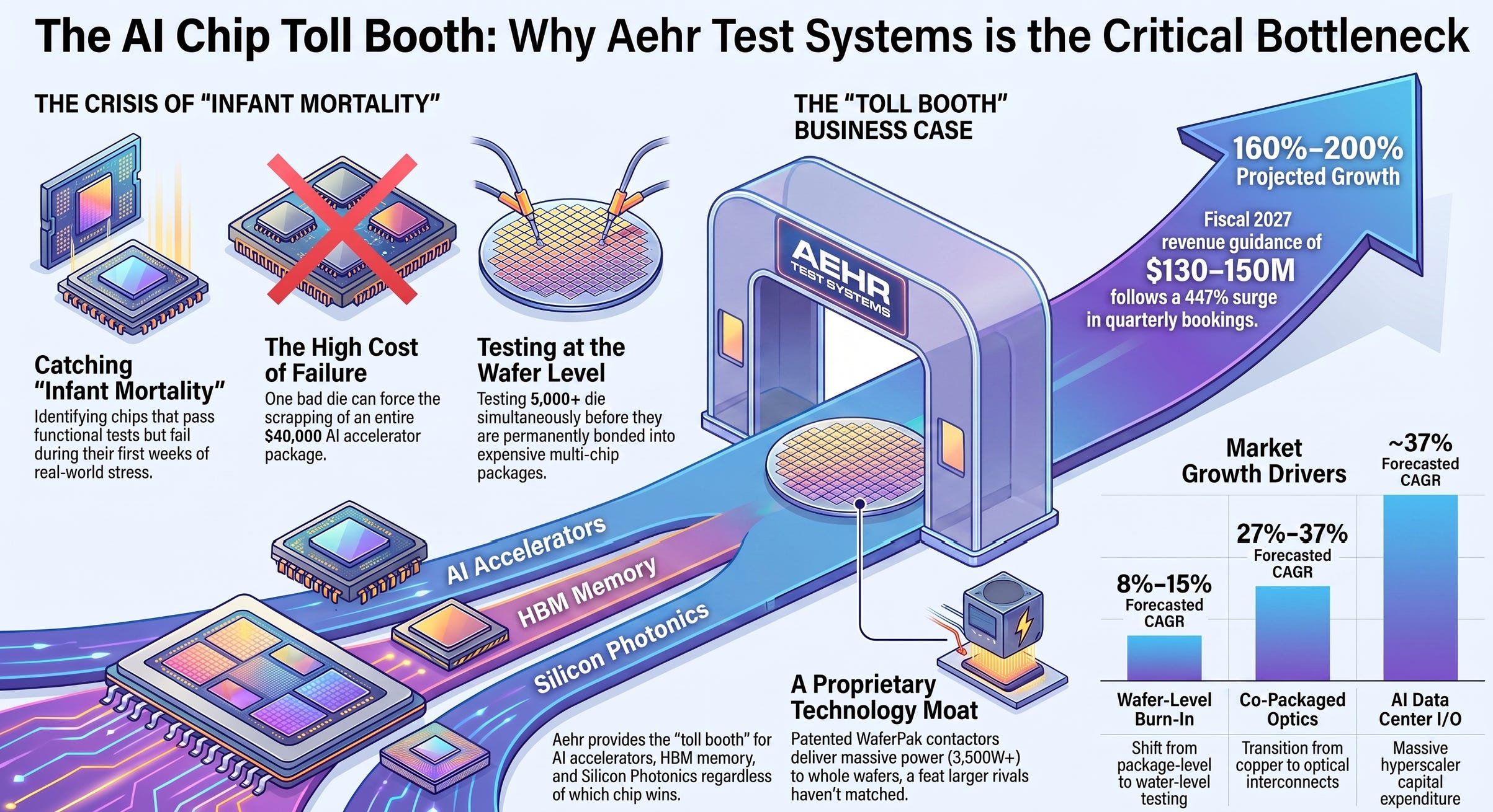
The process is called burn-in. It’s the last quality gate a chip goes through before it gets welded into a $30,000 GPU tray or an HBM stack that’s about to get soldered permanently next to a $40,000 accelerator die. Burn-in exists to catch “infant mortality” — the industry’s actual term for chips that pass every functional test but die anyway in their first weeks of real-world stress. As AI silicon gets more expensive, more power-dense, and more permanently bonded into packages that can’t be reworked, the cost of skipping that gate has gone from “acceptable yield loss” to “scrap an entire multi-die package because one component failed early.” That single dynamic is rewriting who does burn-in, at what stage, and who gets paid for it.
The thesis: Aehr has spent two decades building the only commercially proven way to do burn-in on an entire semiconductor wafer at once, at the power levels modern AI silicon actually needs, and it’s now sitting at the intersection of every major AI hardware trend simultaneously — accelerators, custom ASICs, HBM, the emerging High Bandwidth Flash category, and silicon photonics — without needing to bet on which one wins. The fiscal 2027 guidance management just gave explicitly assumes close to zero contribution from the memory opportunity and doesn’t fully bake in the AI-processor benchmark that just “exceeded the customer’s expectations.” If even one or two of the four separate qualification programs currently in flight convert to high-volume production on the timelines management described, the guide that just sent the stock up 40% could turn out to be the floor, not the ceiling. The timing catalyst is that this isn’t a thesis about the future — the earnings print validating the first leg of it happened yesterday.
Table of Contents
The Market Opportunity
The Core Technology
The Key Bottleneck
The Players Racing to Solve It
The Economics of the Solution
7 Powers Moat Breakdown
The Fallback Scenario
Risks to the Thesis
Conclusion
1. The Market Opportunity
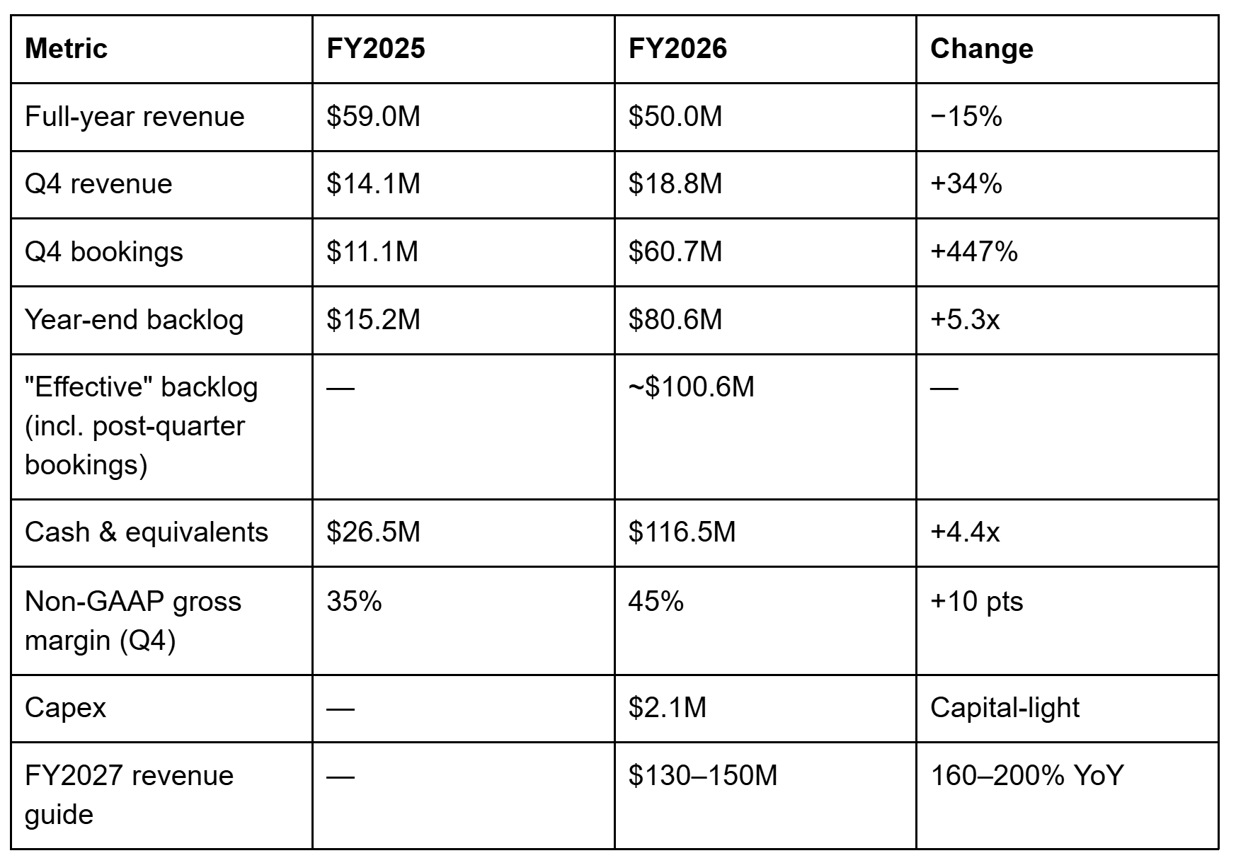
Start with the number management put on paper. Fiscal 2027 revenue guidance: $130–$150 million, implying 160–200% year-over-year growth off a fiscal 2026 base of $50 million. That guide is built on a genuinely unusual foundation — fourth-quarter bookings of $60.7 million (up from $11.1 million a year earlier), a year-end backlog of $80.6 million, and roughly $20 million more booked in the two weeks after the fiscal year closed, bringing the “effective backlog” to about $100.6 million before the new fiscal year had shipped almost anything. Non-GAAP pretax margin is guided to 18–22%.
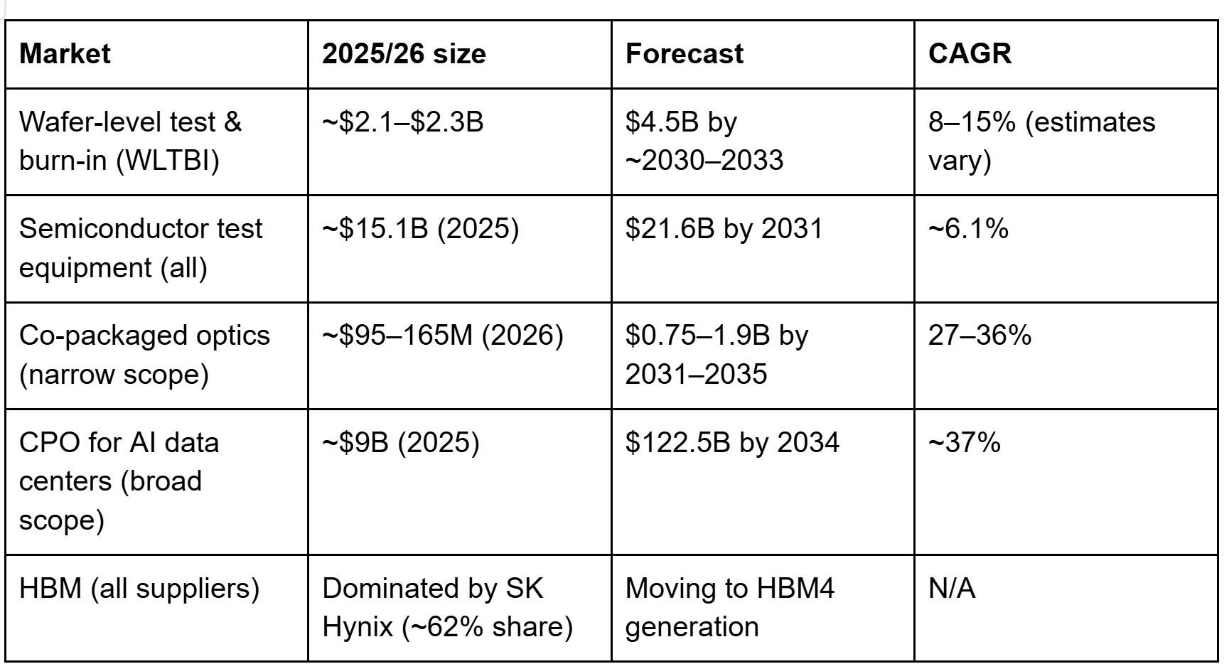
Zoom out from the one company and the setup gets more interesting, not less. The wafer-level test-and-burn-in (WLTBI) niche Aehr operates in is estimated at somewhere between $2.1–$2.3 billion today, with forecasts ranging from a conservative ~8–10% CAGR out to the low-2030s to a more aggressive 14.8% CAGR that would roughly double the market to $4.5 billion by 2030. That’s a small slice of the broader semiconductor test equipment market, pegged at roughly $15 billion in 2025 and growing at a comparatively pedestrian ~6% CAGR — automated test equipment (the Advantest/Teradyne turf) still owns about 70% of that spend, with probe and burn-in equipment as the faster-growing niche riding node scaling and chiplet architectures.
Layer on the two adjacent markets Aehr is actively expanding into. Co-packaged optics and silicon-photonics interconnect forecasts are all over the map — literally three orders of magnitude apart depending on scope, from under $200 million in 2026 by narrow definitions to north of $9 billion once you include the full AI-data-center optical I/O stack, with almost every forecaster converging on CAGRs in the 27–37% range through the early 2030s. That kind of forecasting dispersion is itself informative: this is a market still being defined in real time, not one being carefully measured. And high-bandwidth memory — the category Aehr is trying to break into via its NAND and HBM discussions — sits inside a market where SK Hynix alone commands roughly 62% share, with Samsung and Micron fighting over the rest as the industry pivots to HBM4 and, potentially, an entirely new memory category.
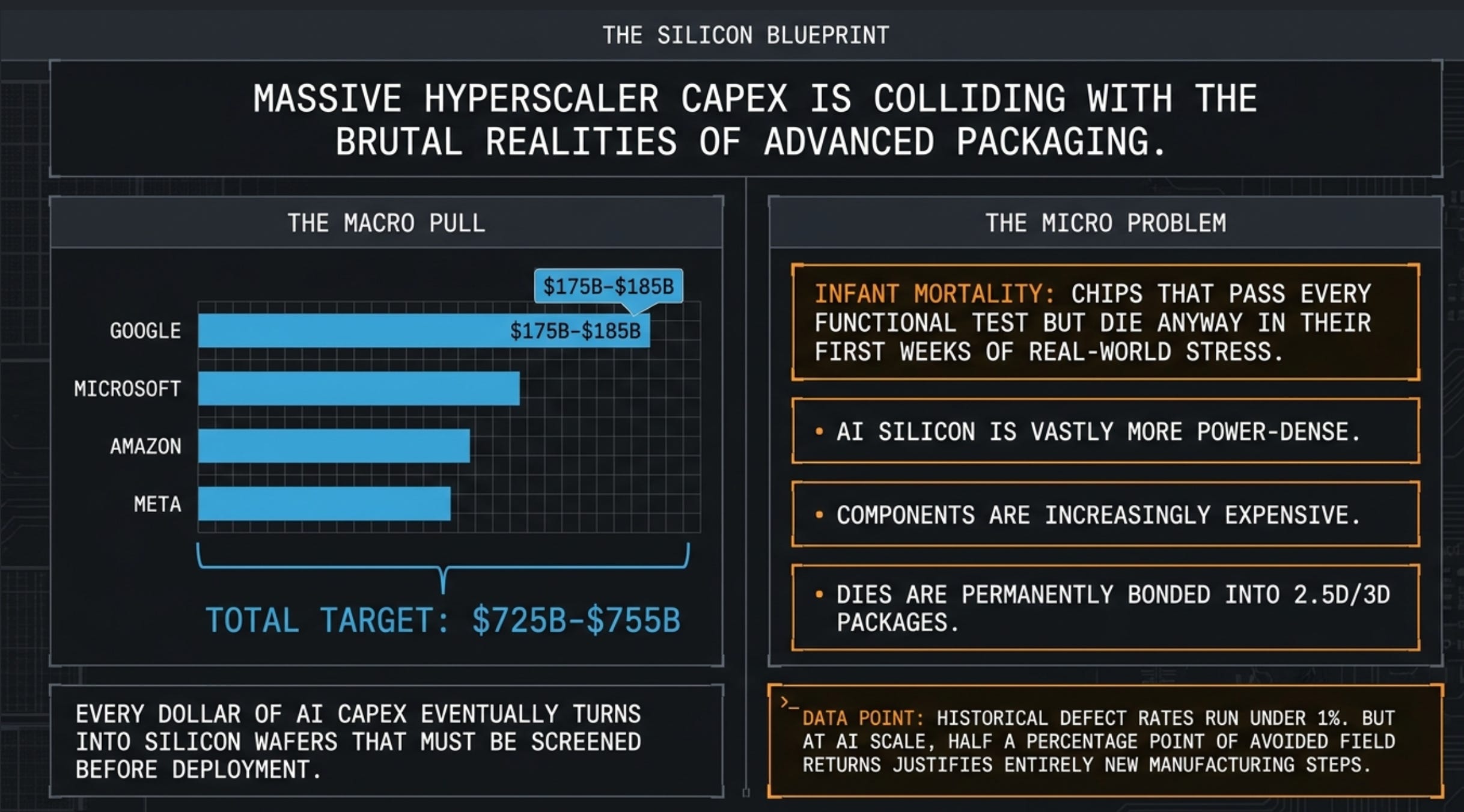
The demand pull underneath all of this is hyperscaler capex, which isn’t really up for debate anymore. Combined 2026 capital spending across Microsoft, Amazon, Google, and Meta is tracking toward roughly $725–755 billion, with Google alone guiding to $175–185 billion. None of that money buys burn-in systems directly — but every dollar of it eventually turns into wafers that need to be screened before they become someone’s data center, and Aehr’s pitch is that it’s one of the very few companies positioned to tax nearly all of it regardless of whose chip design wins.
2. The Core Technology
Burn-in, mechanically, is simple: apply elevated temperature and voltage stress to a device for a sustained period to force latent defects to fail early, before the part ships, rather than three months into service. It’s been part of chip manufacturing since the 1970s. What’s changed is where in the process it happens.
The traditional approach does burn-in at the package level — after a die has already been cut from the wafer, wire-bonded or bump-bonded, and sealed into its final housing. That’s the industry default because it’s simple: you can burn in a tray of finished parts in an oven-like chamber and bin out the failures before they ship. Aehr’s entire business is built around doing the same stress test one manufacturing step earlier — on the whole wafer, before it’s diced, using a proprietary full-wafer contactor called a WaferPak that makes electrical contact with every die on a 300mm wafer simultaneously.
The engineering problem that makes this hard is straightforward to state and brutal to execute: you need to deliver enormous, precisely controlled power to hundreds of individual die spread across a fragile silicon wafer, at temperature, without a single point of contact failing across thousands of pins, for hours at a stretch. Aehr’s FOX-XP platform is specified to deliver up to 3,500 watts per wafer and thousands of amperes of current in its high-power configuration — numbers that sound abstract until you remember that modern AI accelerator packages are themselves pushing 1,000–2,000+ watts, meaning the test equipment has to out-muscle the chip it’s testing. The company’s newer Sonoma platform (acquired via the 2023 purchase of Incal Technology) does the equivalent job at the package level for customers who haven’t yet moved to wafer-level screening, with a newly introduced high-power configuration rated for up to 2,000 watts per device specifically to keep pace with next-generation GPUs and CPUs.
Why do this at the wafer stage at all, given the added complexity? Economics, mostly. If a die fails burn-in after it’s already been packaged — especially in an advanced 2.5D/3D package where several chiplets, HBM stacks, and an interposer have all been bonded together — you don’t just lose that one die, you scrap the entire assembly, including every good component bonded to the bad one. Catching the failure at the wafer stage, before any of that expensive downstream assembly happens, is the entire value proposition. Management’s framing on the recent call was pointed: their AI-processor benchmark customer reportedly told them the wafer-level results were better than what they were achieving at the package level — a notable claim given this is a customer already running mature package-level test programs of its own.
The parallelism is the other half of the value proposition. State-of-the-art wafer-level burn-in configurations are now contacting and stressing well over 5,000 individual die on a single 300mm wafer at once, which is a fundamentally different economic proposition than stepping through packaged parts one tray at a time. That’s also why the WaferPak itself — the physical contactor card that has to make reliable, repeatable electrical contact with every one of those die simultaneously, at temperature, without a single connection degrading over hours of stress — is the actual patent-protected asset here, more so than the FOX or Sonoma chassis that houses it. Aehr has also been building out its go-to-market through outsourced assembly and test (OSAT) partners, expanding relationships with firms like ISE Labs and ASE so that combined wafer-level and packaged-part testing services are available to large semiconductor customers who’d rather buy the service than the capital equipment outright — a secondary channel that widens the addressable customer base beyond companies willing to operate the systems themselves.
3. The Key Bottleneck
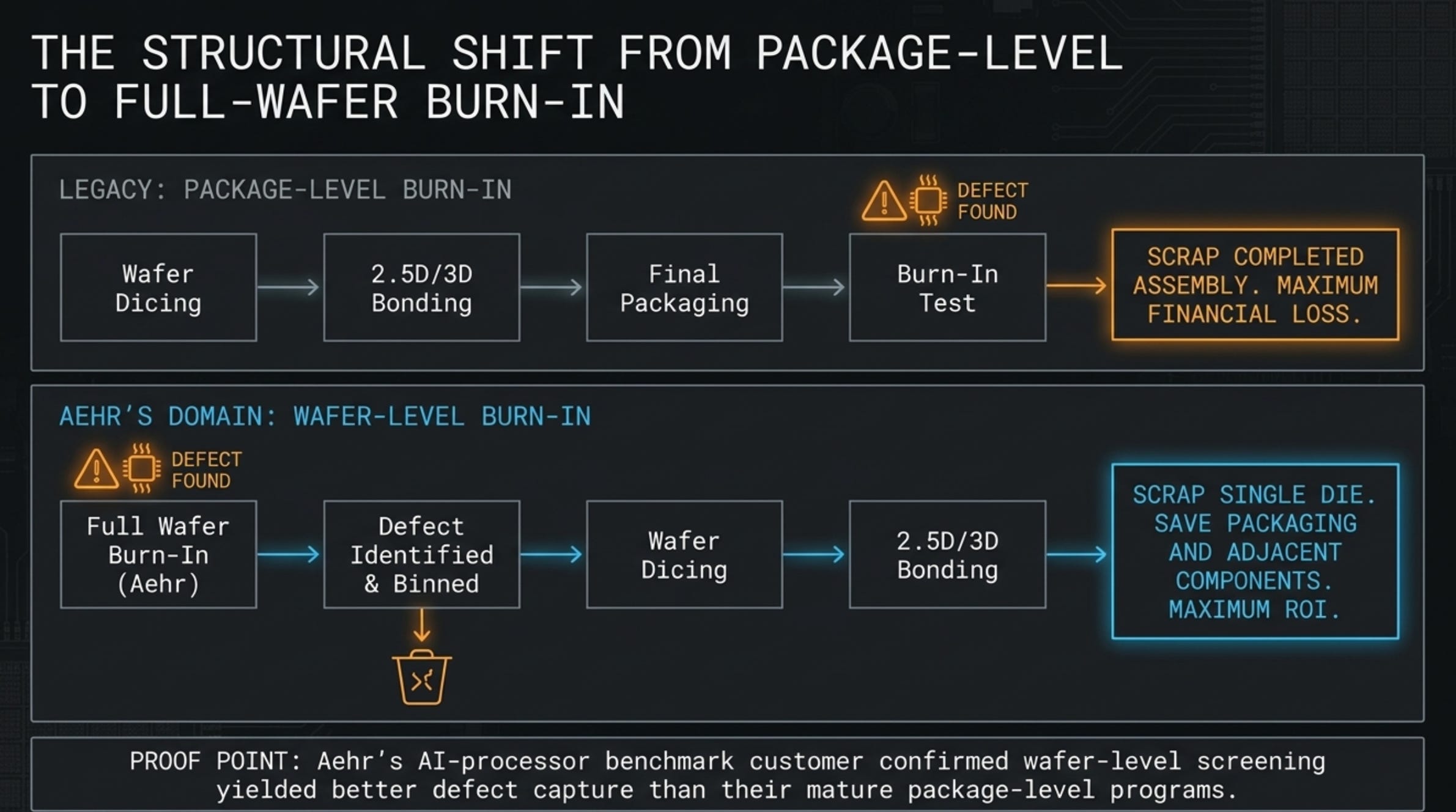
Here’s the thing that makes this a genuine bottleneck rather than just a nice-to-have upgrade: as chip architectures have moved to chiplets, 2.5D/3D packaging, and HBM stacks bonded directly onto accelerator packages, the cost of not catching a defective die before it’s assembled has scaled up faster than the cost of the testing itself. A single bad HBM stack discovered after it’s already bonded to a GPU die doesn’t cost you the price of the memory — it costs you the whole multi-thousand-dollar package. That asymmetry is what’s forcing burn-in earlier in the flow industry-wide, and it’s happening across every device category Aehr touches at once:
AI accelerators and custom silicon. Management said reliability and production burn-in for AI accelerators, CPUs, and network processors was Aehr’s fastest-growing segment in fiscal 2026, at roughly 71% of annual revenue, with AI and photonics combined accounting for more than 80% of fourth-quarter revenue — up from 56% a year earlier. The lead hyperscale customer is reportedly shifting all production burn-in screening to the wafer level, eliminating separate system-level screening entirely, and forecasting a “substantial expansion” of purchases for a second device that draws twice the power of the first.
A second, separately named AI processor supplier — described only as a major supplier of AI accelerators, CPUs, and network processors — just finished a wafer-level benchmark that reportedly exceeded its own expectations, and is now moving toward pilot production validation at a Taiwan-based contract manufacturer, with a second device already requested for parallel evaluation.
Memory. This is the newest and, on the numbers, potentially largest leg. A completed benchmark with an unnamed “global leader in NAND flash” is now in discussions toward a development agreement — one management explicitly ties to next-generation flash and, specifically, High Bandwidth Flash (HBF), the new AI-inference memory category jointly pushed by SanDisk and SK Hynix through the Open Compute Project. Separately, Aehr says it’s in ongoing talks with other major HBM suppliers about aligning test specifications with new capacity coming online. Notably, some new HBM standards are incorporating embedded built-in self-test (BIST) capability, which cuts both ways — it could favor Aehr’s wafer-level architecture, or it could eventually reduce how much external test capacity the industry needs at all. More on that tension in the risks section.
Silicon photonics. As AI clusters shift from copper interconnects to optical ones to solve bandwidth and power bottlenecks, the lasers and photonic integrated circuits driving that shift need their own burn-in — Aehr says it’s the market leader here, with an existing lead customer placing repeat follow-on orders and a brand-new customer (a “global leader in networking products” serving the data-center optical transceiver market) placing its first order in March 2026.
Put together: three customers each represented more than 10% of Aehr’s fourth-quarter revenue — two chasing the AI-processor opportunity, one chasing optical transceivers — and the company describes itself as engaged with “additional AI processor customers” beyond those three. That’s the bottleneck in one sentence: nearly every major category of AI-era silicon now needs a burn-in step that most of the industry still can’t do at the wafer level, and there’s a very short list of companies that can.
The numbers behind “infant mortality” also explain why customers tolerate the added process step at all. On a prior earnings call, management walked through rough failure-rate sensitivity by end market: silicon carbide and gallium nitride power devices have historically shown infant-mortality rates north of 1%, while AI silicon runs under 1% — but even at sub-1% rates, catching roughly half a percentage point of otherwise-undetected failures is enough to prevent a wave of first-year field returns on parts that can cost tens of thousands of dollars per package once assembled. On volumes running into the hundreds of thousands or millions of units a year across a customer’s product line, half a percentage point of avoided scrap and warranty cost is not a rounding error — it’s the entire business case for adding a manufacturing step that, by definition, doesn’t make the chip any better, only more certain.
4. The Players Racing to Solve It
The honest answer to “who’s ahead” is: almost nobody else is racing, because almost nobody else has chosen to compete here directly. The broader semiconductor test equipment market is dominated by Advantest and Teradyne, a long-standing duopoly in automated test equipment (ATE) — the boxes that run functional and parametric tests on singulated die or packaged parts. Both are vastly larger than Aehr (Teradyne generates hundreds of millions in annual free cash flow; Advantest reportedly holds over 5,500 active patents in test-adjacent IP), and both are perfectly capable engineering organizations. Neither, as far as public disclosures show, offers a commercially proven full-wafer, high-power, high-parallelism burn-in system competitive with Aehr’s FOX platform. Cohu and FormFactor sit adjacent — Cohu in test handlers and thermal subsystems, FormFactor and Technoprobe in probe cards — but none of them own the specific full-wafer-contact-at-power niche Aehr has spent decades in. Chroma ATE, a Taiwan-based instrumentation company, is the other name that shows up in burn-in market reports, though with a broader, less AI-specialized product line.
The more interesting competitive threat is regional and legal rather than technological. Aehr is currently suing a Chinese rival — originally named Suzhou Semight Instruments, which has since rebranded and reincorporated in Malaysia as SemiNexus Test (also referred to in filings as “NEXUSTEST”) — for patent infringement on wafer-level burn-in systems targeting silicon carbide devices. Aehr filed the original complaint in a Chinese court in October 2024; on the most recent call, management noted Beijing’s patent office had upheld two of its Chinese patents, a meaningful development given the litigation is still active. Aehr says it beat this same competitor for a new Taiwan-based silicon-carbide customer specifically on technical grounds and reputation — a small but telling data point on how the two are actually competing head-to-head where it counts, on price-sensitive commodity power semiconductors rather than cutting-edge AI silicon.
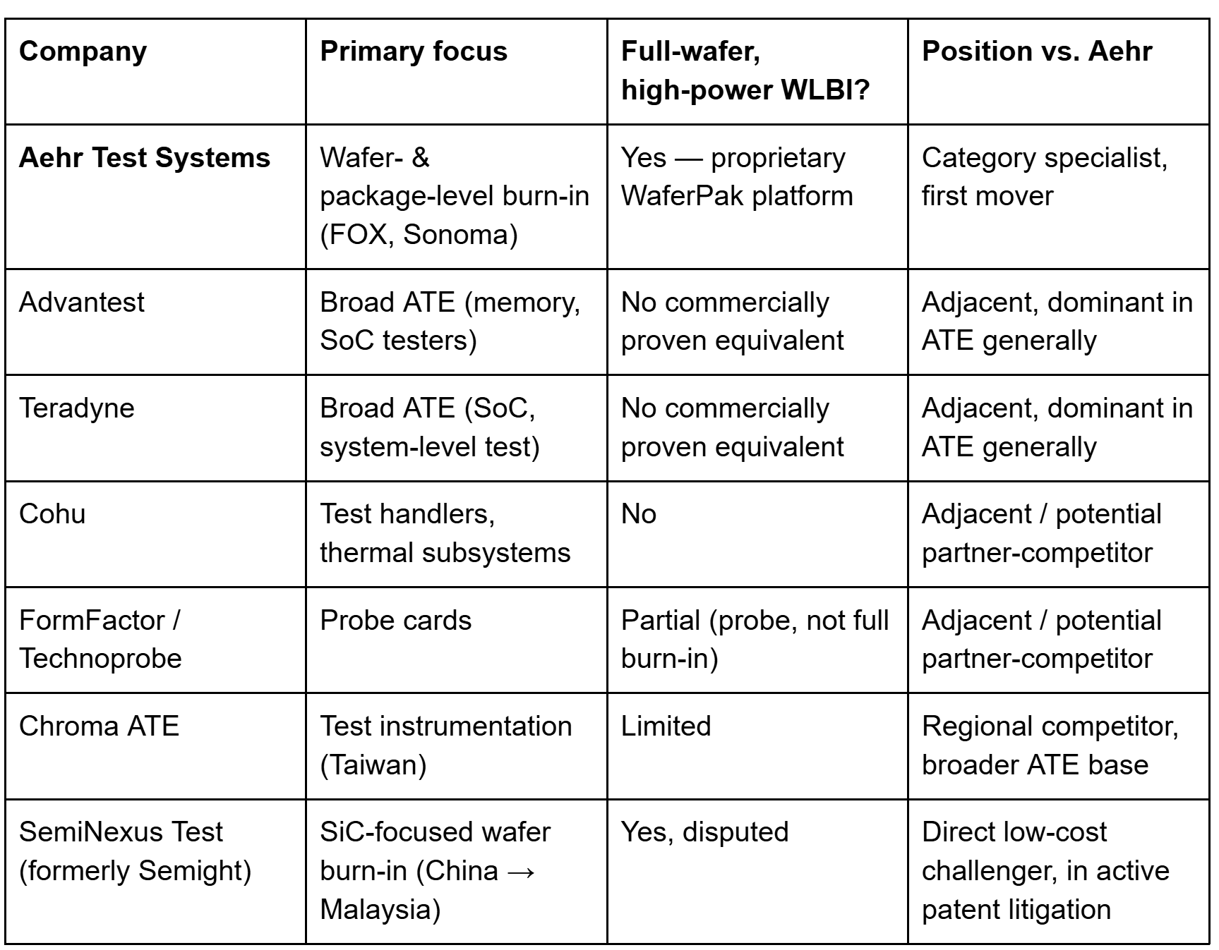
The upshot: Aehr isn’t winning a crowded race so much as running one nobody else has fully entered yet, with the one credible direct challenger currently tied up in a patent fight it appears to be losing on the merits, at least at the Chinese patent office.
5. The Economics of the Solution
The economics here are the part that should make picks-and-shovels investors sit up. Aehr describes a wafer-level burn-in system average selling price of roughly $5–6 million, with system-level gross margins reportedly north of 60%. It’s a genuinely capital-light business on top of that — fiscal 2026 capital expenditures came in at just $2.1 million, and management says its Fremont, California facility (expanded roughly tenfold in recent years) plus a Southeast Asian contract manufacturer together support capacity for roughly 20 combination wafer/package-level systems a month domestically and another 20-plus Sonoma systems a month overseas — capacity management describes as not yet a constraint even at higher guided volumes.
Fourth-quarter non-GAAP gross margin came in at 45%, up from 35% a year earlier, which management attributed to higher revenue, better factory utilization, and a richer mix skewing toward AI and photonics work over lower-margin silicon-carbide business. Full fiscal 2026 revenue landed at $50.0 million (down 15% from $59.0 million in fiscal 2025, reflecting the tail end of the silicon-carbide/EV demand air pocket), with a GAAP net loss of $7.1 million for the year despite the fourth quarter itself turning GAAP-profitable at $1.4 million.
Where it gets interesting for a company this size is the balance sheet reset that happened underneath the operating numbers. Aehr raised roughly $100 million during fiscal 2026, primarily through an at-the-market equity program, taking cash and equivalents from $26.5 million at the end of fiscal 2025 to $116.5 million at the end of fiscal 2026. That’s dilutive, obviously, and worth watching — but it also means a company that used to run close to the edge of its working capital now has real flexibility to fund inventory and consumables ahead of large customer ramps without financing risk becoming the story.
The consumables layer is worth flagging separately: every WaferPak is a per-wafer, per-device-design contactor that needs replacing and re-qualifying as device designs change — a recurring, high-margin revenue stream layered on top of the capital equipment sale, similar in spirit to a razor-and-blades model, except the “blades” here also happen to be patent-protected.
6. 7 Powers Moat Breakdown
Applying Hamilton Helmer’s framework to the three tiers of players in this market — Aehr, the big ATE incumbents, and the Chinese low-cost challenger — makes clear where the real economic protection sits, and where it doesn’t.
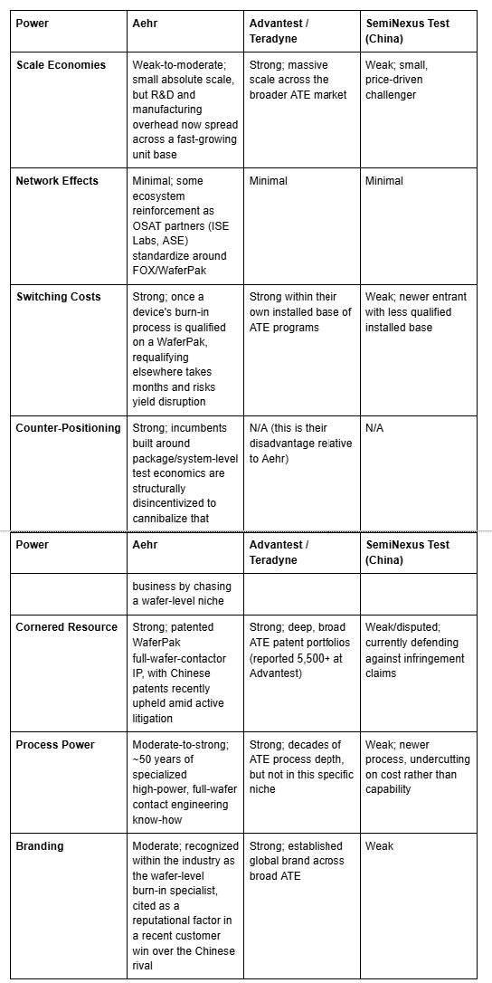
The pattern that jumps out: Aehr’s moat isn’t built on scale (it’s tiny) or branding in the consumer sense — it’s built almost entirely on switching costs, a cornered IP resource, and counter-positioning against much larger rivals who have structural reasons not to chase this specific niche even if they wanted to. That’s a real moat, but it’s also a narrower one than “nobody else can do this” — it’s closer to “nobody else has decided it’s worth doing yet,” which is a materially different, and more fragile, kind of advantage.
7. The Fallback Scenario
What happens if wafer-level burn-in doesn’t convert to high-volume manufacturing on the timelines management is describing? A few plausible paths, none of them catastrophic on their own, but worth sitting with together.
The most benign version: qualification simply takes longer than the 12–18 months management cited for the flash-memory development agreement, or the AI-processor customer’s move from benchmark to “pilot production validation” stretches out, as qualification cycles in this industry routinely do. In that world, Aehr doesn’t lose the business, it just recognizes the revenue later than the backlog math implies — a timing problem, not a thesis problem, but one that would hit a stock already priced for near-flawless execution particularly hard.
A less benign version: package-level and system-level burn-in remain “good enough” for a meaningful slice of the market, and the industry doesn’t fully migrate to wafer-level screening the way the bull case assumes. Memory customers, in particular, have historically used traditional wafer probers from companies like Tokyo Electron or Accretech rather than full-wafer burn-in contactors — Aehr’s own commentary acknowledges its benchmark customer needed convincing that its parallelism and power advantages over those incumbent tools justified switching at all.
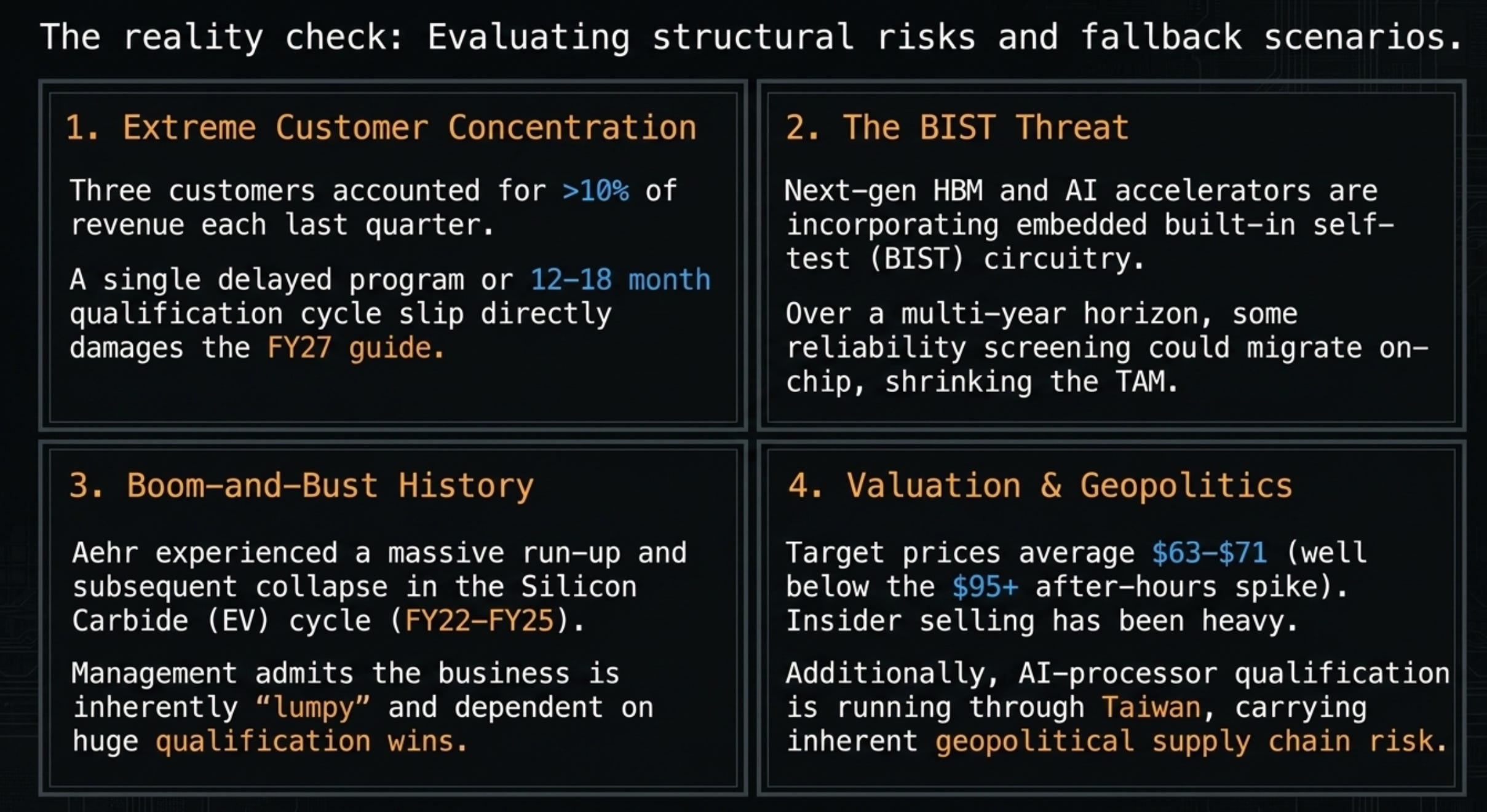
The most structurally interesting fallback ties back to the built-in self-test (BIST) point raised earlier: if next-generation HBM and AI accelerator standards increasingly embed self-test circuitry directly on the die, some of the reliability screening that currently requires external capital equipment could migrate on-chip over time. That’s a slower-moving, longer-horizon risk rather than an immediate one, but it’s the one worth watching over a multi-year holding period rather than a multi-quarter one, since it would shrink the addressable market itself rather than just delaying its arrival.
Finally, there’s the company’s own history as a fallback case study. Aehr has been through exactly this movie once already — its recent past is a boom-bust arc around silicon carbide for EVs, where revenue ran from roughly $50.8 million (FY22) to $65.0 million (FY23) at 50%+ gross margins during the SiC/EV buildout, then slid back down to $59.0 million (FY25) and $50.0 million (FY26) as EV demand cooled and automakers delayed programs. Management’s own framing on the latest call was candid about this pattern, describing the business as inherently “lumpy” given its dependence on a small number of large qualification wins. The AI/photonics ramp is a different, larger market than SiC/EV — but the mechanism by which enthusiasm outruns delivery, then reverses hard, is the same mechanism, and it’s already played out once in this exact stock within the last three years.
8. Risks to the Thesis
Valuation has already run past the fundamentals, on Wall Street’s own numbers. Even after the post-earnings pop, sell-side price targets cluster in the $56–$90 range with an average around $63–$71 — meaningfully below where the stock traded after hours on the print itself. Some independent valuation models put “fair value” dramatically lower still, in the high-teens to mid-$20s, framing the stock as trading several multiples above intrinsic value. That’s not a reason to dismiss the thesis, but it is a reason to separate “the business is executing” from “the stock is cheap” — right now, those are two very different claims.
Customer concentration remains extreme. Three customers accounted for more than 10% of revenue each in the most recent quarter, and the entire fiscal 2027 guide leans on a handful of qualification programs converting on schedule. A single large customer slipping a program, in-sourcing the capability, or simply taking longer than 12–18 months to formalize a development agreement would show up immediately in results at this size.
Insider selling has been heavy into the rally. Multiple sources flag tens of millions of dollars in insider sales over the trailing months with limited offsetting purchases — not disqualifying on its own (insiders diversify for all kinds of reasons after a 4–5x stock move), but a data point worth weighing against management’s own bullish commentary.
Competitive and geopolitical exposure is real, if contained for now. The active Chinese patent litigation could go either direction on appeal, and Aehr’s own AI-processor qualification work is running through a contract manufacturer in Taiwan — a jurisdiction whose semiconductor supply chain sits, as always, adjacent to broader US-China trade and export-control dynamics that have moved unpredictably in both directions over the past year.
The whole setup is a leveraged bet on hyperscaler capex staying uninterrupted. Aehr doesn’t sell to end consumers — it sells into the capital budgets of a handful of chip designers and hyperscalers who are themselves spending several hundred billion dollars a year on the assumption that AI infrastructure demand keeps compounding. Nothing in this piece requires a view on whether that spending environment holds up, but it’s worth being explicit that it’s the load-bearing assumption underneath everything else: a financing-conditions shock, a hyperscaler capex pause, or simply a slower-than-expected AI monetization cycle would hit the qualification pipeline described above well before it hit Aehr’s own backlog math, since customers tend to pause discretionary equipment approvals long before they cancel signed orders.
The guidance itself is a double-edged catalyst. Bookings surging 447% quarter-over-quarter in a single print is a genuinely strong signal, but a book-to-bill ratio that steep also means a chunk of fiscal 2027 revenue recognition is now front-loaded into backlog conversion assumptions that haven’t been tested yet. And because management explicitly said the memory opportunity is not meaningfully baked into guidance, the same fact that makes the upside case exciting also means a chunk of the bull thesis is, by definition, not yet proven out in a single reported number.
9. Conclusion
Strip away the after-hours fireworks and the actual thesis is a fairly simple chokepoint story: as AI silicon gets more expensive per package and more permanently bonded together, the industry has less and less tolerance for finding defects after assembly rather than before it, and there’s a very short list of companies that can move that screening step to the wafer stage at the power levels modern chips require. Aehr currently sits alone at the top of that short list, with patent protection, multi-month-to-multi-year switching costs once a customer qualifies onto its platform, and a customer pipeline that now spans AI accelerators, custom ASICs, silicon photonics, and — if the flash and HBM discussions convert — an entirely new memory category riding the same rails.
What to watch from here, roughly in order of how soon it should show up in the numbers:
The HBF/NAND development agreement — management’s own 12–18 month timeline means the market will have real visibility into whether this converts well before it shows up meaningfully in revenue.
Pilot production validation status for the second AI-processor supplier’s Taiwan qualification — the next disclosed step up from “benchmark exceeded expectations.”
Sonoma second-device ramp at the lead hyperscale customer, given management flagged it as running at roughly twice the power of the first device already in production.
Backlog-to-revenue conversion through the first two quarters of fiscal 2027 — the single cleanest test of whether the bookings surge was real demand or timing noise.
The China patent litigation docket — a durable win there reinforces the cornered-resource moat; a reversal opens the door to the one credible low-cost challenger.
Whether sell-side price targets ever catch up to the stock, or whether this remains a situation where the fundamentals and the valuation are simply having two separate conversations.
None of that requires picking a winner between Nvidia and its challengers, or between HBM and HBF, or between pluggable optics and co-packaged optics. That’s the actual edge here — and also exactly why a 40% single-day move on a stock this size shouldn’t surprise anyone. When the market can’t agree on how to value the toll booth, it tends to re-price it violently every time new traffic data comes in.
Disclaimer: This is not financial or investment advice. This piece is for informational and educational purposes only, reflects publicly available information as of July 15, 2026, and should not be relied upon as the basis for any investment decision. Markets, guidance, and litigation outcomes can change quickly. Do your own research, consult a licensed financial advisor, and size any position according to your own risk tolerance.